Pong Sound
This article goes through the circuit schematics of classic arcade game Pong from 1972, and analyzes how its sound is generated.
Table of contents:
A Warm-Up Exercise
[1]
Atari was founded in June 27 1972 by Nolan Bushnell and Ted Dabney.
Around 1971, the company (then known as Syzygy Engineering) hired Allan Alcorn, who had just finished his Bachelor degree in electrical engineering and computer science [2]. Atari boss Nolan Bushnell assigned him the task of creating a tennis game, as a 'warm-up exercise'. Except for a prototype of Bushnell's 'Computer Space', Alcorn had never seen a video game before. [3]
After two months, Alcorn had finished 'Pong'. Bushnell decided that the game was good enough to try producing and selling. In June 1972, the arcade cabinet started production, and ended up selling 35,000 units, generating a profit of 17.5 m$. [4]
All Hardware, No Software
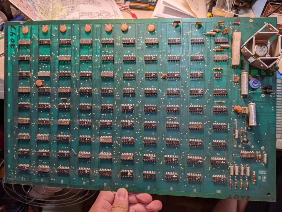
Pong is 100% implemented in discrete logic hardware, no CPU, no software.
Pong is implemented using Transistor-Transistor Logic (TTL) integrated circuits (ICs), which were invented in 1961 and first manufactured in 1963. They are small chips with 14 or more pins, and they perform simple logic operations such as a Not-And operation (NAND), retaining a few bits of memory, binary counting, or a timer. Pong was implemented using the Texas Instruments 7400 series of TTL chips.
Here are some of the TTLs used in Pong:
--------------------------------------------------------------------------
List of Pong components

Part #   Function
--------------------------------------------------------------------------
TTL ....................................................................
7400     NAND
7404     NOT
7410     3-input NAND
7430     8-input NAND
7474     2xflip flop (2 x 1-bit memory)
74107    2xflip flop with clear
7493     4-bit binary counter (divide by 2, 4, 8)
9316     4-bit up/down binary counter

Other ..................................................................
555      2.1 MHz timer
--------------------------------------------------------------------------
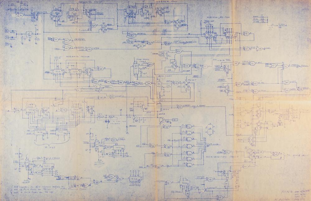
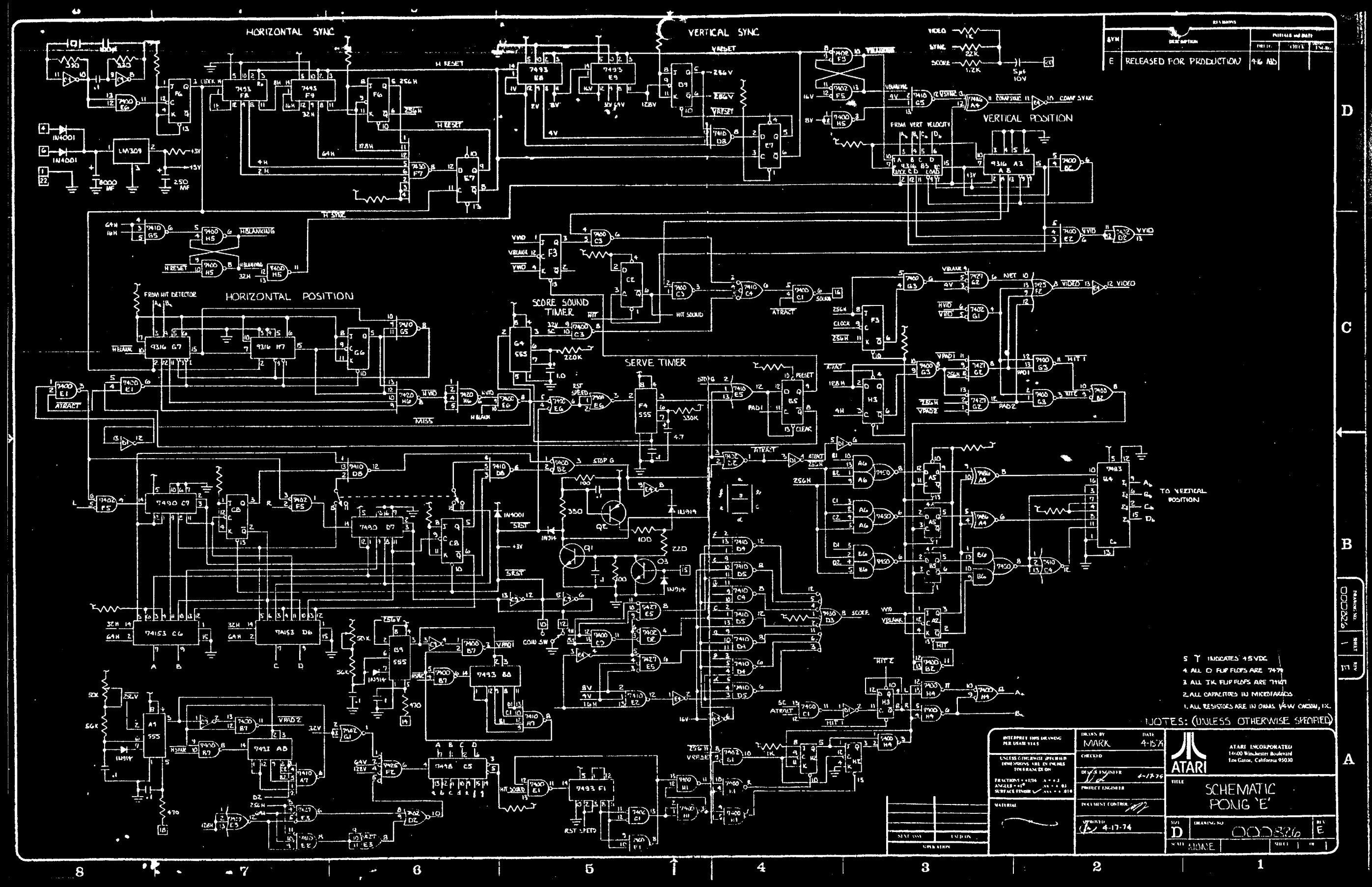
The whole game is contained on a single board with 66 TTL chips and a few more components.
[5]
The game runs from a master clock at 7.1575 MHz, synchronously controlling everything, including game logic, reading control input, rendering graphics, and finally generating video and audio output signals.
Video and sound is generated digitally. The sound is 1-bit mono and consists of 3 different sound effects: 'hit', 'bounce', and 'score'.
The video is internally 1-bit as well, but when output, a difference in resistance at the final stage creates a difference in brightness between the score numbers, and the rest of the graphics.
The game has an attract mode (refered to in the diagrams as) ATRACT, which changes the behaviour of the game and disables all sound.
I wanted to investigate how the sound worked, but to understand that, I need to understand the signals that generated the sound, which turned out to be video synchronization counters. To understand those, I worked my way through the basic synchronization circuits, which I will attempt to explain in the following.
Synchronization
To output black and white video to a CRT display using a composite video signal, you need to output a correctly timed horizontal synchronization pulse (HSYNC) that tells the CRT to start a new scanline and a correctly timed vertical synchronization pulse (VSYNC) that tells the CRT to start a new frame. Between these sync pulses you output a luminance signal that represents the black and white image. When the HSYNC and VSYNC happens, the luminance should go black (horizontal and vertical blanking intervals), to avoid drawing artifacts while moving the electron beam.
First, we will investigate how Pong generates HSYNC and VSYNC signals.
We start out with the circuit that generates the master clock for Pong.
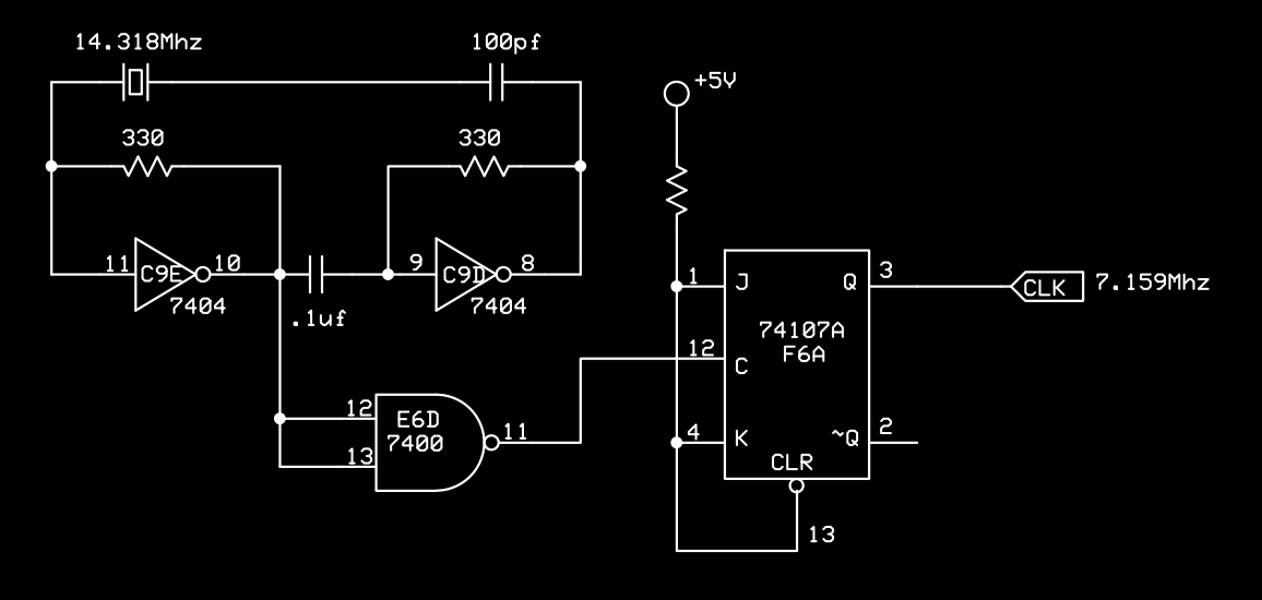
It's based on a 14.318 MHz crystal, 7404 inverters, 330 Ohm resistors, a 100 pF capacitor, and a 7400 NAND gate wired as an inverter. Supposedly, this is a standard setup to generate a stable clock, although the exact workings are beyond me. [6] [7]
However, after this point, we can start to analyze the purely digital operation in the right side of the diagram:
- The 14.318 MHz signal is routed through a 74107A flip-flop.
- C triggers the flip-flop operation on a falling edge (meaning the input goes from 1 to 0).
- At that moment, the previous state of J, K, and CLR yields the result output from Q and ~Q.
- The output of the 7400 is routed to all the J, K, and CLR inputs, so they are all 1 at this point.
So what does it mean when J, K, and CLR are all 1, on the falling edge of CLK?
We can consult the Function table for the 74107A (see the reference) for what happens in this case:
-------------------------------------
Input               Output
~CLR  CLK   J  K    Q  ~Q
-------------------------------------
  1   neg   1  1    toggle
-------------------------------------
neg: triggered on negative-edge pulse
     i.e. going from 1 to 0
The output Q (and the inverse ~Q) are toggled. So the output of the flip-flop toggles on every input, generating a square wave signal at half the input signal, at:
14.318 / 2 MHz = 7.159 MHz
From this point on, we have CLK, a 7.159 MHz master clock that controls the timing of everything else in Pong, including the audio.
HRESET
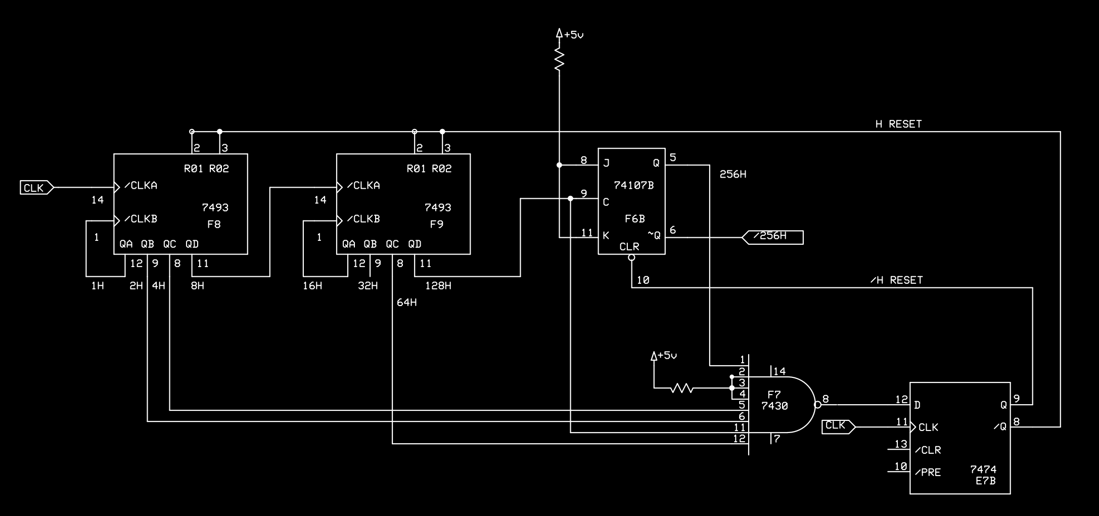
CLK is routed through two 7493 4-bit counters and a 74107B flip flop which together act as a 9-bit counter that increments every time CLK goes high.
Let's look at the first 7493 counter (F8). First how it's set up:
- Since QA is connected to ~CLKB, it works as a 4-bit counter.
- R01 and R02 are connected to HRESET, the output of this whole circuit.
- Our master clock CLK is fed into ~CLKA, which triggers counting one value up.
- The internal count value is represented as four binary digits in QA-QD.
Thus, F8 counts the number of times the input CLK goes high:
          _     _     _     _     _
clock  __| |___| |___| |___| |___|
         :     :     :     :     :
       0000  0001  0010  0011  0100
The binary digits can be accessed through individual pins, which can be seen in this table, where the binary counter value is shown vertically, with QA containing the least significant bit and QD the most significant bit:
CLK        0101010101010101010101010101010
QA (1H)  | 0 1 0 1 0 1 0 1 0 1 0 1 0 1 0 1
QB (2H)  | 0 0 1 1 0 0 1 1 0 0 1 1 0 0 1 1
QC (4H)  | 0 0 0 0 1 1 1 1 0 0 0 0 1 1 1 1
QD (8H)  | 0 0 0 0 0 0 0 0 1 1 1 1 1 1 1 1
The most significant bit is used as the clock input for the second 4-bit counter (F9) which thus ends up counting the next 4 bits in a combined 8-bit counter:
CLK  (8H)  | 001111111100000000111111110000000011111111 (condensed)
QA  (16H)  | 0 1               0               1
QB  (32H)  | 0 0               1               1
QC  (64H)  | 0 0               0               1
QD (128H)  | 0 0               0               0
128H is transfered to a '74107' flip-flop (F6B). It is configured in 'toggle mode' (J=K=1), which sets Q high every other pulse. This forms the 9th bit of a combined 9-bit counter (256H).
If not reset, this 9-bit counter will count CLK inputs from 0 to 511.
The 7430 at the bottom right (F7) is an 8-input NAND gate, which is 1 unless every input is 1. Inputs 2-4 are connected directly to 5V, so they are always 1, and the 5 other input pins get their input from binary counter digits 2H and 4H from the first 4-bit counter, 64H and 128H from the second 4-bit counter, and 256H from the flip-flop. These are true when we have counted up to:
2 + 4 + 6 + 128 + 256 = 454
This sets the D input on a 7474 flip flop, which on the next CLK pulse which enables HRESET. This HRESET happens on the CLK pulse after the 454th that we counted up to, so it'll happen on the 455th CLK pulse.
HRESET resets the two 4-bit counters, and ~HRESET resets the negative-edge CLR on the 76107 flip-flop. This resets the count to 0.
Now, the loop restarts and thus, HRESET is triggered every 455 CLK pulses. HRESET represents the time when the CRT beam switches to a new scanline.
Since we know the master CLK frequency (7.159 MHz), we can compute the frequency that HRESET occurs at:
7.159 MHz / 455 = 15.73 KHz
HRESET is used for horizontal CRT beam synchronization. Now, let's look at VRESET and vertical CRT beam synchronization.
VRESET
The HRESET signal is used as a clock input to generate the vertical reset signal (VRESET), which signals the CRT to move the electron beam to the top and draw a new screen.
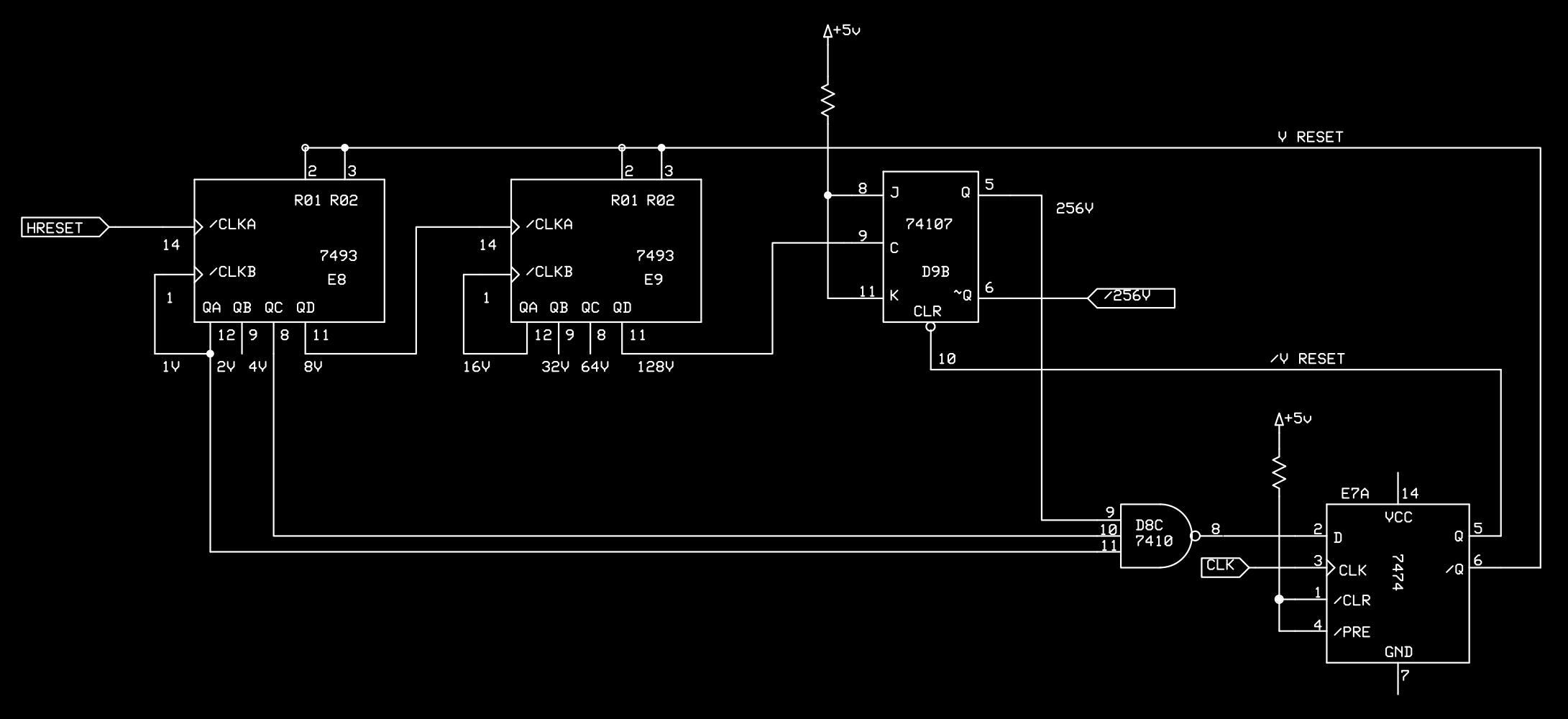
It works the same as the combined 9-bit counter used to generate HRESET, except the 7410 3-input NAND waits for the pins 1V, 4V, and 256V to be set, which happens after 261 steps:
1 + 4 + 256 = 261
The 7474 flip-flop then waits for the next CLK, with the result is that VRESET gets triggered every 262 HRESET pulses, generating 262 scanlines.
The 32V bit output of the second 4-bit counter is used for sound. It's worth considering what the output of a counter looks like. The input signal for the first 4-bit counter is HRESET, which only last a single CLK cycle. So they are short pulses, like so:
          _         _         _         _
HRESET __| |_______| |_______| |_______| |_______
However, if the input has a fixed frequency, the output from the binary counters are square waves, regardless of the pulse width. This can be seen in this example:
CLK    000100010001000100010001000100010001000100010001000100010001 | F
QA  | 0   1   0   1   0   1   0   1   0   1   0   1   0   1   0   1 | F/2
QB  | 0   0   1   1   0   0   1   1   0   0   1   1   0   0   1   1 | F/4
QC  | 0   0   0   0   1   1   1   1   0   0   0   0   1   1   1   1 | F/8
QD  | 0   0   0   0   0   0   0   0   1   1   1   1   1   1   1   1 | F/16
The output from Qx are all square waves. So we know that the 32V output from binary counter E9 is also a square wave at 1/64 the frequency of HRESET. The frequency of 32V is:
f(32V) = f(HRESET) / 64
       = 15.73 KHz / 64
       = 245.8 Hz
However, since the counter is reset every 262 CLKs, the square wave is 'glitchy'.
 pulse len 32 32  32  32  32  32  32  32  32+4 32
              ___     ___     ___     ___      ___
          ___|   |___|   |___|   |___|   |_*__|
 counter  0  32  64  96  128 160 192 224 256

                                           0   32
VPOS16 and VPOS32
For reasons that are not entirely clear, two signals from the ball vertical counter circuit are used for sound together with the aforementioned 32V.
The ball vertical counter is implemented using a separate counter that runs at the same frequency as the VRESET counter, but is offset. According to [8], this employs Nolan Bushnells US Patent 3,794,383 "Video image positioning control system for amusement device". [9]
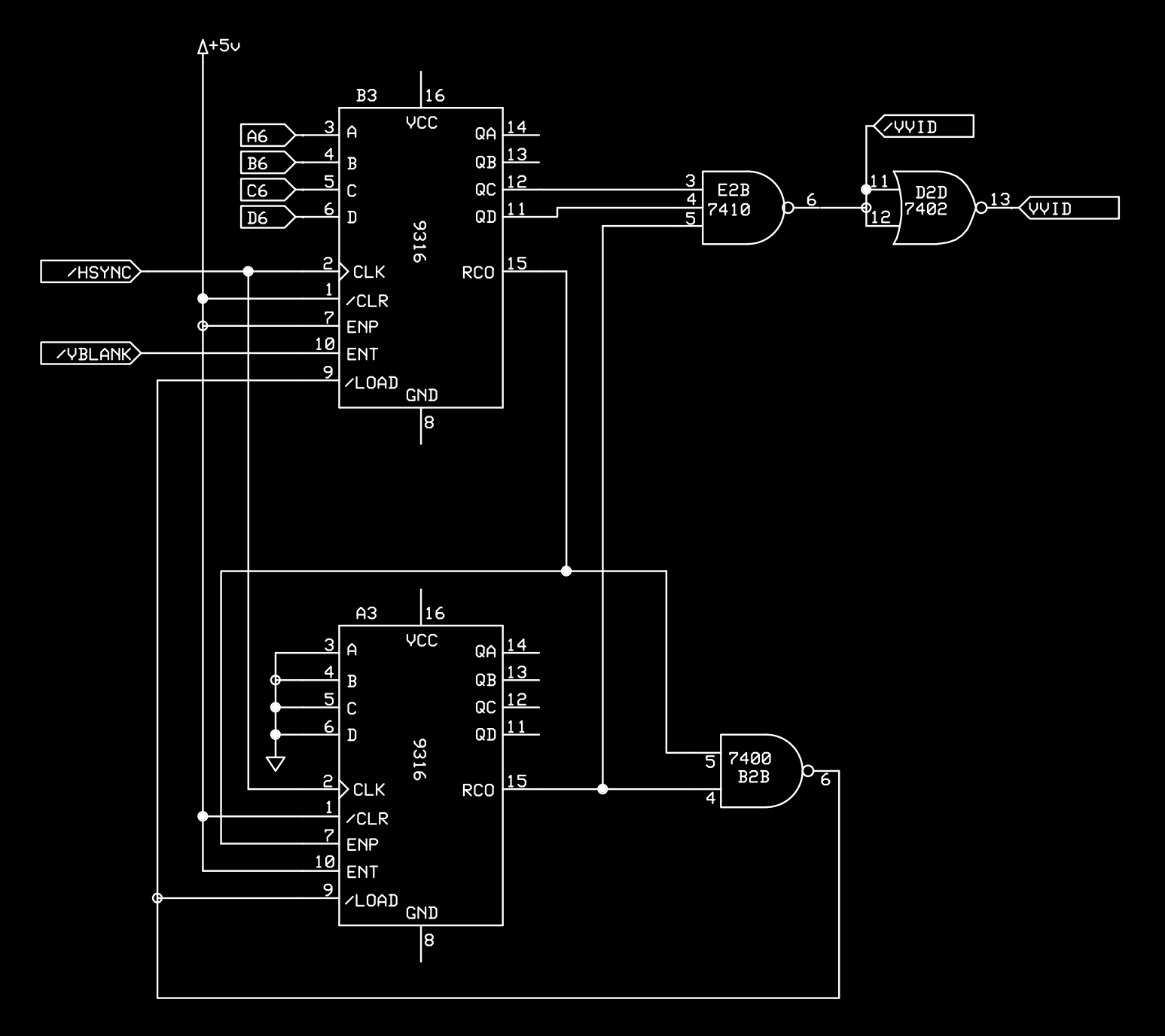
Without going into further detail, we can see that HSYNC (which triggers at the same frequency as HRESET) is used as a clock for updating the ball position.
HSYNC is counted using 2 4-bit counters connected in a multistage counting configuration (see 9316 documentation p6) - why this circuit is using different counting circuits is unclear to me.
However, what we are interested in are the two digits VPOS16 and VPOS32, which run at the same frequencies as 16V and 32V, that is
f(VPOS16) = f(HRESET) / 32 = 591.6 Hz
f(VPOS32) = f(HRESET) / 64 = 245.8 Hz
Since 32V and VPOS32 both are square waves at the same frequency, it is confusing why Alcorn wouldn't just use one of them. The reason might be one of print layout convenience, and Alcorn also stated that the sound implementation was done in half a day after the rest of the board was finished:
Now the issue of sound ...People have talked about the sound and I've seen articles written about how intelligently the sound was done and how appropriate the sound was.
The truth is, I was running out of parts on the board. Nolan wanted the roar of a crowd of thousands—the approving roar of cheering people when you made a point. Ted Dabney told me to make a boo and a hiss when you lost a point, because for every winner there's a loser.
I said, "Screw it, I don’t know how to make any one of those sounds. I don’t have enough parts anyhow." Since I had the wire wrapped on the scope, I poked around the sync generator to nd an appropriate frequency or a tone. So those sounds were done in half a day. They were the sounds that were already in the machine.
[10]
Sound Circuit
We now have the signals that are used for generating sound:
--------------------------------------------------------------------------
Sound-related Signals
--------------------------------------------------------------------------
VPOS32  245.8 Hz square wave
VPOS16  591.6 Hz square wave
32V     245.8 Hz square wave
--------------------------------------------------------------------------
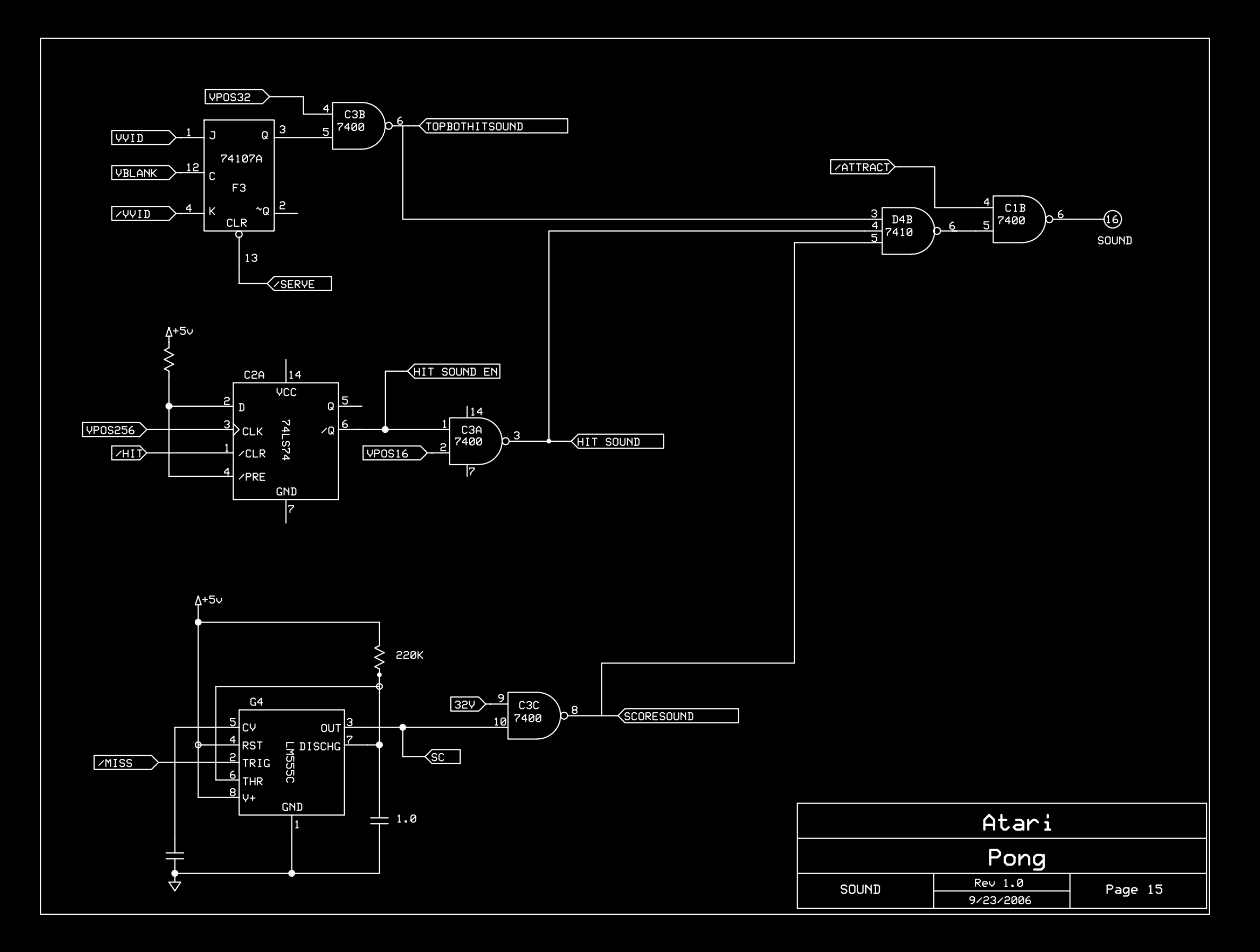
In the diagram we can see the 3 different sounds, noted
TOPBOTHITSOUND
HIT SOUND
SCORESOUND
They all output their signal into D4B, a 3-input NAND (7410), which goes high if any input is low and low otherwise, effectively 'mixing' the digital inputs together.
The mixed signal is ANDed with /ATTRACT, which means that we're not in attract mode. So the sound is muted when in attract mode.
The final digital output is sent directly to the sound output.
Now, let's investigate each of the 3 sounds.
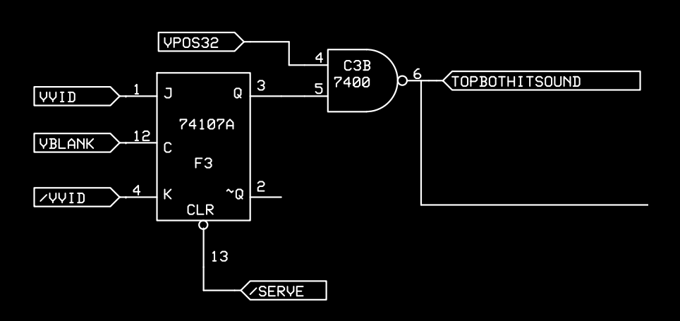
VVID is high if the ball is currently active in the current scanline.
HVID is high if the ball is the vertical pixel column currently being drawn.
If HVID and VVID are both high, the ball is drawn - a white rectangle.
If VBLANK is high, we are in the vblank area under or over the playfield.
TOPBOTHITSOUND is triggered when VVID and VBLANK are both high at the same time, meaning that the ball is intersecting the VBLANK area, i.e. hitting the top or bottom.
When this event happens (and we're not in /SERVE mode), the F3 flip flop goes high, and the VPOS32 signal is routed to the D4B 'mixer'. As soon as the ball moves out of the VBLANK area, the flip flop is disabled again. Playing the game, I believe this happens the frame immediately after the ball hits the top or bottom. It should be verifiable in the vertical ball control.
A single frame worth of 245.8 Hz square wave will be heard as a result.
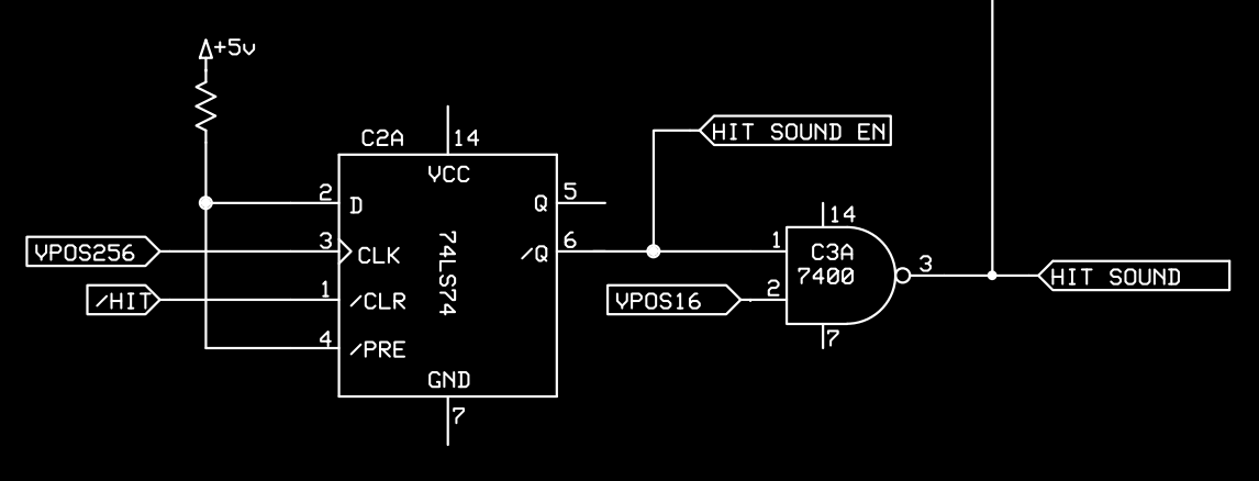
The 7474 flip flop controlling the hit sound is normally high, and is pulled low by the /HIT signal clearing it. This results in /Q enabling VPOS16 being output to the 'mixer'.
It only gets updated once every frame by being CLK'ed with VPOS256.
A single frame worth of 591.6 Hz square wave is the result.
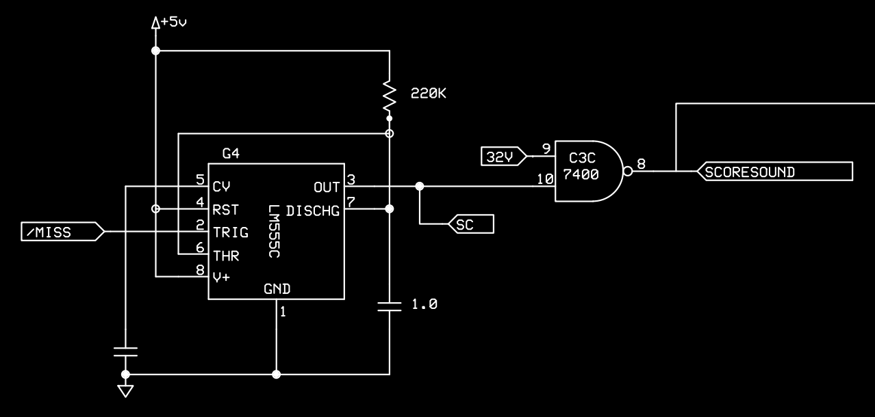
Finally, the SCORESOUND is triggered by the signal /MISS when the ball goes beyond the paddles horizontally. This triggers a 555 timer that goes high for 242 ms, which is used as a gate that enables 32V to be sent to the 'mixer'.
This results in a 242 ms 245.8 Hz square wave.
TTL Chips
TTL 7404 : Hex Inverters
Y = ~A

------------------
Truth table

Input Output
A     Y
------------------
0     1
1     0
------------------
[11]
TTL 7400 : Quad 2-input NAND gate
In the Pong schematics, we only see a single NAND gate in use, although several parts of the circuit could in theory use different gates on the same TTL chip.
Y = ~(A and B)

------------------
Truth table

Input Output
A  B  A NAND B
------------------
0  0  1
0  1  1
1  0  1
1  1  0
------------------
[12]
TTL 7410 : Triple 3-input NAND gate
This is a 3-input NAND gate that implements
Y = ~(A and B and C)
Y =  ~A or ~B or ~C

----------------------
Truth table

Input    Output
A B C    Y
----------------------
1 1 1    0
0 X X    1
X 0 X    1
X X 0    1
----------------------
[13]
The 7410 contains 3 separate of these 3-input NAND gates.
TTL 7430 : 8-input Positive-NAND Gates
A 8-input NAND gate that implements
Y = ~(A and B and C and D and E and F and G and H)
Y =  ~A or ~B or ~C or ~D or ~E or ~F or ~G or ~H

----------------------
Truth table

Input         Output
A-H             Y
----------------------
All inputs 1    0
One+ input 0    1
----------------------
[14]
TTL 7474 : Dual Flip-Flops
---------------------------
Function table

Input               Output
/PRE /CLR CLK   D   Q  /Q
---------------------------
  0    1   X    X   1   0
  1    0   X    X   0   1
  0    0   X    X   1   1
  1    1   pls  1   1   0
  1    1   pls  0   0   1
  1    1   0    X   Q0 /Q0
---------------------------
pls: triggered on pulse
     i.e. going from 0 to 1
[15]
TTL 74107A : Dual Flip-Flops with Clear
Stores a single bit (and its inverse) in Q and /Q.
On CLK, the J and K inputs are used to either set or toggle the stored bit.
-----------------------------------
Function table

Input               Output
~CLR  CLK   J  K    Q  ~Q
-----------------------------------
  0    X    X  X    0   1
  1   neg   0  0    Q0 ~Q0
  1   neg   1  0    1   0
  1   neg   0  1    0   1
  1   neg   1  1    toggle
  1    1    X  X    Q0 ~Q0
-----------------------------------
neg: triggered on negative-edge pulse
     i.e. going from 1 to 0
It seems that there is no functional difference between 74107A and 74107B, although I have not been able to confirm it.
TTL 7493 : Four-bit Binary Counter
              CKB -+-----+- CKA <- clock input
     reset -> R01 -+     +- NC
       "   -> R02 -+     +- QA  <- binary digit #1
              NC  -+     +- QD  <- binary digit #4
              VCC -+     +- GND
              NC  -+     +- QB  <- binary digit #2
              NC  -+-----+- QC  <- binary digit #3
VCC is +5 V positive supply voltage, GND is ground.
To use as a 4-bit counter, QKB must be connected to QA.
If both reset pins (R01 and R02) are high, the binary digits are reset to 0.
---------------------------
Function table

Reset inputs       Output
R01 R02      QD  QC  QB  QA
---------------------------
1     1      0   0   0   0
0     X      --- COUNT ---
X     0      --- COUNT ---
---------------------------
Otherwise, the 7493 counts up from 0000 to 1111.
---------------------------
Count Sequence

        Output
COUNT   QD  QC  QB  QA
---------------------------
  0     0   0   0   0
  1     0   0   0   1
  2     0   0   1   0
  3     0   0   1   1
  4     0   1   0   0
  5     0   1   0   1
  6     0   1   1   0
  7     0   1   1   1
  8     1   0   0   0
  9     1   0   0   1
 10     1   0   1   0
 11     1   0   1   1
 12     1   1   0   0
 13     1   1   0   1
 14     1   1   1   0
 15     1   1   1   1
---------------------------
[16]
LM555 Timer
[17]
HSYNC
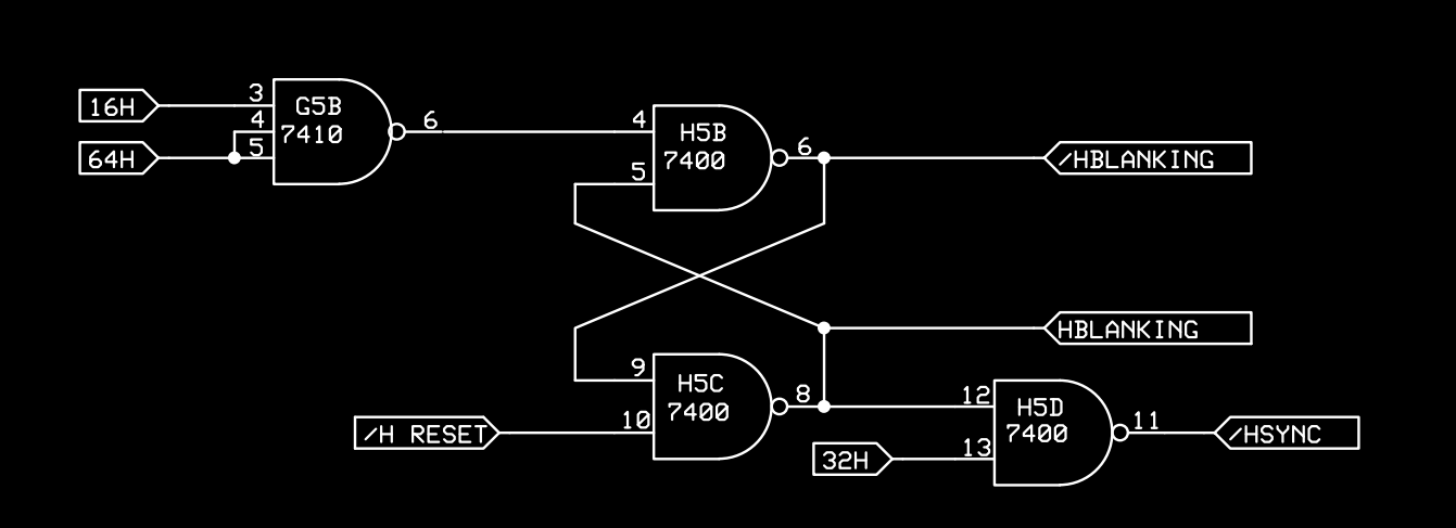
The 7410 NAND gate G5b goes low when 16H and 64H are high. This corresponds to reaching horizontal pixel 80.
When /HRESET goes low, both 16H and 64H are also low.
In this circuit, the horizontal synchronization signal HSYNC is generated at the same frequency as HRESET, but offset. HSYNC is generated by HBLANK and 32H, and cleared by HRESET. Both happen once per scanline.
! FIXME: better explanation
References
-
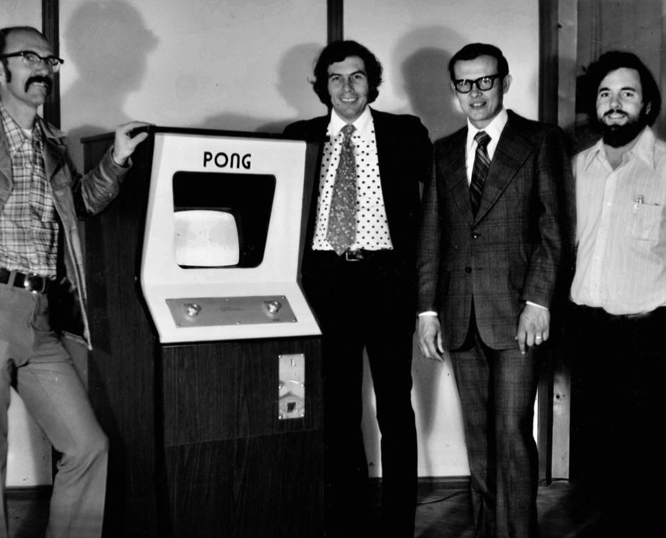
Atari founders Ted Dabney and Nolan Bushnell with Fred Marincic and Al Alcorn
Al Alcorn (1972)
From computerhistory.org ↩ -
We can read in [3] that Alcorn had not seen a video game except
for a prototype of 'Computer Space', which was entering production in
November-December 1971. ↩ -
Pong at 50: the video game that ‘changed the world’
The Week (Nov 29 2022)
theweek.com ↩ -
Pong PCB - What do these components do?
Reddit user DicCheyney (2022)
reddit post
reddit.com ↩ -
Pong
Dan Boris (2007)
Annotated Pong schematics, IC list, dev blog
tech bloch atariage.com
Pong main page atarihq.com ↩ -
Pong schematics
Dan Boris (2006)
Annotated Pong schematics
Pong schematics atarihq.com ↩ -
Reconstructing Pong on an FPGA
Stephen A. Edwards (December 2012)
Department of Computer Science, Columbia University
Great article that carefully explains through the Pong circuits
PDF Article ↩ -
Video image positioning control system for amusement device.
Nolan K. Bushnell (February 1974)
US Patent US-3793483-A (search for patent # 3793483) ↩ -
The Ultimate History of Video Games
Steven L. Kent (2001)
Prima Publishing ↩ -
SN7404 etc. Hex Inverters
Texas Instruments (2026)
Texas Instruments datasheet ↩ -
SN7400 etc. Quadruple 2-Input Positive-NAND Gates
Texas Instruments (2026)
Texas Instruments datasheet ↩ -
SN7410 etc. Triple 3-Input Positive-NAND Gates
Texas Instruments (2026)
Texas Instruments datasheet ↩ -
SN7430 etc. 8-input Positive-NAND Gates
Texas Instruments (2026)
Texas Instruments datasheet ↩ -
SN7474 etc. Dual D-Type Positive-Edge-Triggered Flip-Flops with Preset and Clear
Texas Instruments (2026)
Texas Instruments datasheet ↩ -
SN7593A, etc. Decade, Divide-by-Twelve and Binary Counters
Texas Instruments (2026)
Texas Instruments datasheet ↩ -
Signetics Linear Vol 1 Data Book
Signetics (1972)
Signetics ↩